3D silicon nanopatterns with extremely smooth surface

© 2018 EPFL
Congratulations to Yuliya Lisunova and co-authors for their publication in Microelectronic Engineering "Combination of thermal scanning probe lithography and ion etching to fabricate 3D silicon nanopatterns with extremely smooth surface".
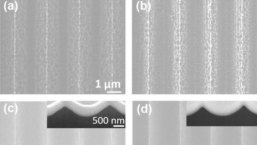
An emerging and extremely enabling route towards rapid prototyping of complex topographies with nanoscale precision and with highly controlled surface position is thermal scanning probe lithography. This technique, coupled to the recent advances in dry etching, allows pattern transfer into the target material at high vertical amplification and could therefore provide access to novel devices. However, the dry etch processing used to transfer the resist pattern into the structural material results in pronounced surface roughening, ultimately diminishing the functional quality of the nanostructures. To access the area of applications such as nano-photonics, nanoelectronics, nano-mechanics and nano-fluidics to name a few, a better control of surface morphology down to the sub-nm scale is a key request. Here, we explore different ion-beam polishing techniques for the surface roughness reduction of thermal scanning probe lithography patterns in silicon. Direct ion beam etch was optimized to smoothen thermal scanning probe lithography features and further extended to a polymer mask technique. The critical step of introducing the polymer mask for the ion beam etching enables extremely smooth three-dimensional surface contours at a sub-nanometer surface roughness.